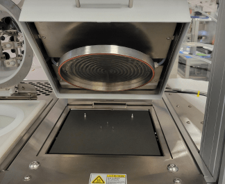
Our client faced persistent issues with photoresist delamination during the photolithography process. To address this, we implemented a solution involving Hexamethyldisilazane (HMDS) priming using the Apogee® 200mm Bake Plate. This enhanced photoresist adhesion, improved yield, reduced defects, and lowered costs, ultimately streamlining project timelines. Additionally, a 75° contact angle was achieved within a 90-second process, showcasing the success of the solution.
Facing challenges with inconsistent adhesion of photoresist in the photolithography process, the client encountered persistent issues with photoresist delamination. Initial process optimizations included surface preparation, testing different photoresists, and modifying process parameters, with no positive outcomes. As a consequence, they continued to experience reduced throughput, increased expenses, rework, and delayed project timelines. In order to establish a durable bond between the substrate and the photoresist, the wafer surface was prepped with HMDS before the coating.
A review of the client’s existing process included an analysis of the following potential causes:
The root cause of the poor adhesion was identified as inadequate bonding of the photoresist due to absorbed water in the silicon wafer from ambient humidity. A simple dehydration bake was inadequate to resolve the issue. The use of hexamethyldisilazane (HMDS) chemical vapor deposition (CVD) was proposed for use before the application of photoresist.

HMDS priming enhances the substrate surface for photoresist adhesion through the formation of a hydrophobic monolayer, reducing surface energy to ensure uniform coating. This layer also prevents air entrapment, enhancing photoresist wetting and minimizes defects during photolithography.
The Apogee® 200mm Bake Plate served as the ideal foundation to accommodate the client’s substrate sizes. The standard bake process model was modified to include the following and then installed into the X-Pro II Workstation:
• vacuum chamber hood with an HMDS inlet
• pressure can with HMDS bubbler for vaporization
• control box with specialized valves
• recipe-controlled process parameters via Datastream™ software
Operational Flow:
1. Set the bake plate to the desired temperature.
2. Initiate vacuum inside the chamber to commence the initial dehydration bake.
3. Nitrogen pre-purge to eliminate oxygen from the chamber.
4. Introduce HMDS vapor to the chamber, promoting the formation of a monolayer on the wafer.
5. Apply vacuum to the wafer to bake off residual HMDS and displace remaining water molecules.
6. Nitrogen post-purge, ensuring complete removal of HMDS from the chamber.
A contact angle measurement provides important insight into the HMDS process. For photoresist coating, a measurement between 60-90 degrees is typically desired for proper wetting and adhesion. Unfortunately, a standard silicon wafer is measured at only ~40 degrees. The application of HMDS, brings the contact angle into the acceptable range.
With this implementation, the customer was able to demonstrate a 75 degree contact angle which led to a marked improvement in:
• Photoresist Adhesion
• Throughput (90 second process)
• Minimized Defects
• Decreased Rework
• Yield
Project timelines were reduced, promoting efficiency and a reduction in costs.
Substrate Sizes
pieces
2″
3″
100mm
150mm
200mm
Technical Details
Vacuum Chamber: >24 inHg vacuum
HMDS canister with tube-controlled bubbler from 0-10 lpm
Rotameter-controlled pre/post inert (N2) gas purge, controlled from 0-5 lpm
Temperature range up to 180°C
Recipe controlled via Datastream™ software
Materials
hexamethyldisilazane
silicon & silicon oxide wafers